Attopsemi’s I-fuse OTP Passed 3 lots of HTS and HTOL Qualification for 1,000hr on GLOBALFOUNDRIES 22FDX FD-SOI Technology
Attopsemi’s I-fuse™ provides small size, high reliability, low program voltage/current, low power and wide temperature to enable GLOBALFOUNDRIES 22nm FDX® for AI, IoT, automotive, industry, and communication applications
Santa Clara, California — April 1, 2019
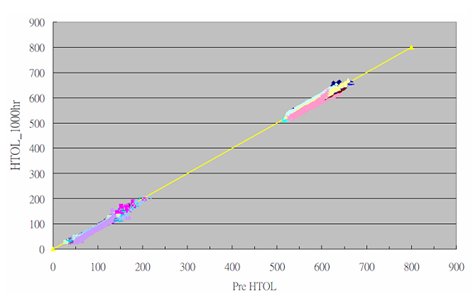
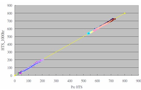
Attopsemi, an OTP IP provider, announced today that the company’s 256Kb OTP (One-Time Programmable) IP, manufactured on GLOBALFOUNDRIES (GF®) 22FDX® technology, passed 3 lots of 150°C HTS and and 125°C HTOL for 1,000 hours following the JEDEC standards. Not only all 120Mb in 3 lots of HTS/HTOL passed functionally, the cell currents did not show any variations after stresses. The defect rate is less than 0.01ppm. This is a phenomenon as most other OTPs show severely parameters shifted and tailing bits after HTS/HTOL stresses. The X/Y plots of cell current in post-stress versus pre-stress are shown in the followings:
“Other than high reliability, I-fuse™ can be programmed at 1.0V with only 1.0mA of program current, said Shine Chung, Chairman of Attopsemi, “Because of no need for charge pumps, our I-fuse™ OTP size can be only 1/4 to 1/5 of the competing OTP technologies.” “Moreover, I-fuse™ can work at wide temperature range of from -55oC to 150oC without needing any redundancies, ECC, or twin cells.” Our I-fuse™ also offers high data security and full testability unseen in any other OTPs.” This IP also passed 250oC HTS wafer-level burn-in in a previous press release.
“We sincerely appreciate all the support from GF in developing our proprietary I-fuse™ OTP technology on 22FDX,” said Shine Chung, Chairman of Attopsemi. “After many years of dedicated works and collaboration with foundries and customers worldwide, our I-fuse™ technology has finally been demonstrated as OTP of choice. We have proven that I-fuse™ can ensure high reliability with smaller size by using a fraction of program current. With our superior OTP IP, we expect to bring substantial benefits to all semiconductor communities.”