• I-fuse® Silicon-Proven

    on FinFET Tech

    Press ReleaseWebinar
  • I-fuse® OTP

    meet AEC-Q100 grade 0
    with zero failure return.

    Read more
  • Super Small and Scalable

    Innovated S3 architecture helps surpass all others

    Read more
  • I-fuse®

    Revolution
    non-Explosive
    Fix all problems in OTP

    Read more

I-fuse®

non-explosive OTP

Attopsemi I-fuse® OTP is one-time programming memory IP with patented I-fuse® which is fully standard logic process design, without extra mask or special processes steps.

I-fuse® is the innovative design and is not as anti-fuse technology; thus the OTP does not need charge-pump and has been qualified from 0.7 µm to 22 nm.

Comparing to other existing OTP solutions, Attopsemi OTP is an easy-to-use OTP which offers customer’s product the outstanding competitiveness with the fully testability and the leading performance, such as high reliability, no need redundancy, extreme compact size, low program/read voltage, low power consumption and wide temperature range of operation.

Achievement

Patent

90+ patents granted
USA 72+ /TWN 8 /CN 10 /UK 1
3+ fuse types 5+ variations

Technology

meet AEC-Q100 Grade 0+
Silicon Proven 12nm – 180nm
N12 qualified in Q1 2023

Cooperation

150+ customers embedded
10K shipped wafers
Zero failure return

Patent

90+ patents granted
USA 72+ /TWN 8 /CN 10 /UK 1
3+ fuse types 5+ variations

Technology

meet AEC-Q100 Grade 0+
Silicon Proven 12 nm – 0.7 um
N12 qualified in Q2 2023

Cooperation

150+ customers embedded
10K shipped wafers
Zero failure return

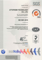
ISO:9001 Certificate

Your QMS is very well organized and controlled, and your ISO9001 certification is well earned.

Feedback from the first–tier North America customer after audit

Target Market

Attopsemi I-fuse® OTP is an optimal fit that provides maximum design flexibility toward customer’s product; the IP passes the qualification of the AEC-Q100 grade zero level reliability, targeting a variety of applications in advanced automotive, industrial, and medical applications.

Use Case

High Reliability

HTS:300°C,4Khr 110nm
HTS: 250°C, 1Khr 22nm

Small Size

4Kbits0.031mm228nm
2Kbits0.045mm222nm

Low V PGM

2Kbits PGM 1.1V 22nm
2Kbits PGM 1.1V 40nm

Low Energy Read

512bits Read V: 1.5V–5.5V  130nm
1Kbits Read V: 0.81V–1.32V 55nm

High Reliability

HTS: 300°C, 4Khr 110nm
HTS: 250°C, 1Khr 22nm

Small Size

4Kbits 0.031mm2 28nm
2Kbits 0.045mm2 22nm
(PGM 1.1V w/ CP)

Low V PGM

2Kbits PGM 1.1V 12nm
2Kbits PGM 1.1V 22nm
2Kbits PGM 1.1V 40nm

Low Energy Read

256bits Read V: 1.5V
current: 3uA 180nm
1Kbits Read V: 0.81V–1.32V 55nm

Latest News

© 2022 Copyright - Attopsemi® Technology Co., Ltd.
- made by bouncin